Silicon
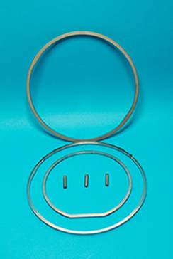
INDUSTRIAL SILICON - RAW & MACHINED
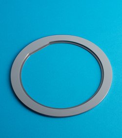
SILICON MACHINING
Silicon can come as Monocrystalline silicon (or single crystal silicon) and Polycrystalline silicon (polysilicon or poly-si). Silicon is often used as the primary base material that silicone microchips and semiconductors are made from; which can be found in virtually all electronics. The material is also a key component in solar cells as the substance acts as a strong light absorbing material.
Silicon is a safe, highly adaptable material well suited for any number of electronic or light-related environments or applications. It’s a stable, reliable performer that is also affordable, making it one of the most common manufactured materials.
MONOCRYSTALLINE SILICON
Monocrystalline silicon is a crystalline structure, or crystal lattice, is one continuous solid with no breaks and is free of grain boundaries with no impurities. This gives monocrystalline silicon an advantage over virtually all other materials – an ability to reliably deliver desired performance specifications across highly complex devices such as microprocessors. It can be doped with small amounts of other elements to deliver specific semiconductor performance characteristics.
Monocrystalline silicon for industrial applications is created in a laboratory in large ingots that are later machined or ground into the proper shape and size for a particular application.
POLYCRYSTALLINE SILICON
Polycrystalline silicon is a manufactured silicon material that is comprised of many small silicon crystals. The semiconductor and solar cell industries are the primary uses of polycrystalline silicon due to its ability to be manufactured to near pure state. This purity is critical in creating efficient solar panels.
Polycrystalline silicon manufacturers create the material in large blocks or rods that are broken into smaller pieces for further machining into thin slices. The slices are further machined into a thinner sheet for production of semiconductor components or photovoltaic cells.
Polycrystalline silicon is known to be highly conductive and operate efficiently at high temperatures. These properties make the material ideal for MOS transistor gate electrodes and interconnections in a MOS transistor circuit. It is also commonly used for resistors and other integrated circuit applications.
For solar cell applications, the less perfect surface of the polycrystalline silicon means it absorbs less light than monocrystalline silicon. This inefficiency results in larger photovoltaic cells. However, polycrystalline silicon is less expensive and easier to produce than monocrystalline silicon photovoltaic cells.
Applied Ceramics has the experience necessary to precisely grind and machine silicon into a number of shapes, sizes, and forms to exacting tolerances. Our skilled technicians have the experience in machining silicon for semiconductor and solar cell applications. If you’re looking for a reliable and trusted silicon wafer manufacturer with the know-how to produce components to your specifications, Applied Ceramics would be proud to be your trusted silicon and ceramic machining provider.
In addition, we can perform silicon micromachining for intricate shapes and details such as channels and etchings. We achieve this by using the latest laser and CNC equipment to build microstructures by deposition and etching of different structural layers on top of the substrate. The result is a component that is ready for production or R&D prototyping.
We also offer raw silicon in a variety of purities, shapes, and quantities.
Contact an experienced Applied Ceramics professional to discuss your silicon machining application, learn more about the silicon manufacturing process and work together to design and deliver the parts you need to your desired specifications.
APPLICATIONS
- Semiconductors and microchips
- Semiconductor devices (MOS transistors, integrated circuits, resistors)
- Solar cells
- High power laser optics
MAIN PROPERTIES
- High Purity: Free of grain boundaries for a pure substance free of impurities
- Light absorbing (photovoltaic)
- Stable in a number of environments
- Can be polished
- High thermal conductivity, from cryo up to 1100°
-
Silicon
Properties Units Silicon MECHANICAL Density g/cm3 2.33 Color – gray Water Absorption % 0 Flexural Strength MPa@room temp.(R.T.) – Compressive Strength MPa@R.T. – Hardness GPa 11.3 THERMAL Coefficient of Linear Thermal Expansion 1E-6/°C
(»25°C to Ј1000°C)2.3-2.6 Thermal Conductivity W/m°K@R.T. 125 Specific Heat cal/g°C@R.T. 0.18 Thermal Shock Resistance D T(°C) – Maximum Use Temperature °C 1350 ELECTRICAL Volume Resistivity Ohm. cm@R.T. 0.005->20 Dielectric Constant 1MHz@R.T. 11.7